Cleanroom Systems: The Backbone of Semiconductor Manufacturing
In the fast-evolving semiconductor manufacturing industry, precision is everything. Every microchip and electronic component must be manufactured under the strictest conditions, where even a single speck of dust can cause a defect. This is where cleanroom technology comes into play.
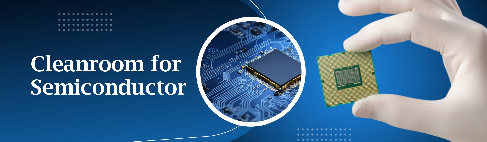
A cleanroom semiconductor is a highly controlled environment designed to eliminate dust, airborne particles, and chemical vapours. These advanced setups ensure the flawless production of semiconductors, protecting the delicate fabrication process from contamination. Without cleanroom for semiconductor manufacturing, achieving high yields and product reliability would be nearly impossible.
The Role of Cleanroom Technology in Semiconductor Manufacturing
Cleanroom technology is the foundation of semiconductor manufacturing. Companies invest heavily in these systems to maintain the highest level of cleanliness, precision, and efficiency. But what makes semiconductor cleanroom design so important?
Here are the key components that define a well-optimized cleanroom system:
Advanced Air Filtration
High-Efficiency Particulate Air (HEPA) and Ultra-Low Particulate Air (ULPA) filters remove microscopic particles, ensuring ultra-clean air circulation.
Precision Temperature & Humidity Control
Semiconductors are highly sensitive to environmental changes. Controlled temperature and humidity levels prevent static build-up and defects.
Strict Contamination Control
The personnel working here must follow strict semiconductor cleanroom standards, including wearing protective suits and passing through air showers to prevent contamination.
Electrostatic Discharge (ESD) Protection
Semiconductor components are prone to damage from static electricity. Cleanrooms incorporate ESD-safe flooring and ionization systems to mitigate risks.
By implementing an advanced semiconductor cleanroom system, semiconductor manufacturers can maintain industry compliance, improve production efficiency, and reduce costly defects.
Key Factors in Semiconductor Cleanroom Design
A semiconductor cleanroom design requires careful planning and adherence to industry standards like ISO 14644. The goal is to create an environment where contamination risks are minimized, and operational efficiency is maximized.
1.
Proper Airflow & Filtration
Cleanrooms rely on laminar airflow systems that direct filtered air in a uniform manner. This prevents airborne contaminants from settling on sensitive surfaces.
2.
Use of Cleanroom-Grade Materials
The materials used in cleanroom construction must be non-shedding, chemical-resistant, and easy to clean. Common choices include stainless steel, epoxy-coated surfaces, and seamless flooring.
3.
Strict Entry & Exit Protocols
Workers must pass through airlocks, gowning areas, and high-efficiency filtration zones before entering the cleanroom. This ensures no external contaminants are introduced.
4.
Automation & Monitoring Systems
Modern cleanrooms integrate real-time environmental monitoring, automated air purification, and contamination detection to ensure optimal conditions are maintained at all times.
Why Investing in Cleanroom Systems is a Smart Move for Semiconductor Companies
For semiconductor manufacturers, the decision to invest in high-quality cleanroom systems is not just about compliance but also it’s about staying ahead in a highly competitive industry. A well-designed semiconductor cleanroom enhances product reliability, reduces waste, and improves overall production efficiency.
With rapid advancements in semiconductor technology, companies that prioritize cleanroom technology will have a significant edge in terms of quality, yield, and innovation. Whether you’re setting up a new fabrication facility or upgrading your existing setup, starting looking for a cleanroom semiconductor supplier is essential for long-term success.
How FTS Cleanrooms Can Help You Build a World-Class Semiconductor Cleanroom Facility
Being the best semiconductor cleanroom company, we at FTS Cleanrooms specialize in designing and constructing state-of-the-art systems for semiconductor manufacturing and assembly facilities. Our team of experts understands the semi-conductor cleanroom classification, and associated unique challenges of contamination control, and provides turnkey solutions tailored to meet your exact requirements.
Here’s how FTS Cleanrooms can support your project:
Customized Cleanroom Design
We are one of the trusted cleanroom semiconductor companies, as our designs comply with ISO 14644 and meet the highest industry standards. Our layouts optimize airflow, contamination control, and operational efficiency.
Advanced HVAC & Filtration Systems
We implement cleanroom technology that ensures precise temperature, humidity, and particulate control for sensitive semiconductor fabrication processes.
ESD Control Solutions
Our cleanroom designs incorporate ESD-safe flooring, grounding systems, and ionization solutions to prevent electrostatic discharge, protecting delicate microelectronics.
Modular & Scalable Construction
Whether you need a small assembly area or a large-scale fabrication facility, our modular cleanroom solutions can be customized to fit your growing needs.
Regulatory Compliance & Validation
Our cleanrooms are designed to align with global industry regulations, ensuring seamless certification and validation for your semiconductor production facility.
With a proven track record of delivering high-performance cleanroom systems across the MENA region, FTS Cleanrooms is your trusted partner for setting up a contamination-free semiconductor cleanroom. We cater to markets in the UAE, Saudi Arabia, Kuwait, Qatar, Oman, Bahrain, Yemen, and African countries.
Telephone: +971 65772230
Mobile & WhatsApp: +971 50 213 6044
Email: [email protected]