
The Ultimate Guide to Semiconductor Cleanroom Design
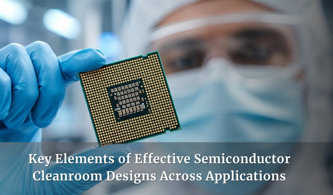
A pharmaceutical cleanroom and a semiconductor cleanroom can both be ISO Class 7. However, they can still fail to meet each other’s basic needs. Semiconductor cleanroom design has to account for something most controlled environments never think about: static electricity. A speck of dust ruins a pharmaceutical batch. A tiny electrostatic discharge can destroy a microchip that costs more than the room it was built in.
That’s the core difference driving everything else in this piece. Designing a semiconductor cleanroom has specific needs. These needs change based on your focus. It could be wafer fabrication, packaging, testing, or something else.
What Is Cleanroom Validation?
Semiconductor cleanrooms need to manage electrostatic discharge (ESD) as well as airborne particles. Even a tiny static charge can damage a microchip, which isn’t something particle contamination can do.
In pharma or food production, contamination risk is almost entirely about particles and microbes. Keep the air clean, keep surfaces sanitized, and you’ve covered most of the risk.
Semiconductor manufacturing adds a layer most other industries never deal with. Static charge builds up from everyday actions. This includes materials touching and separating, like wafers and containers or gloves and panels. It also happens when air moves across surfaces. That charge doesn’t need to touch a product to damage it. A discharge in the nanojoule range can ruin a chip’s tiny circuits. Often, there’s no visible damage at first. The device may only fail later in the field.
That’s why a semiconductor cleanroom isn’t just a tighter version of a pharma cleanroom. Good semiconductor cleanroom design starts with a unique primary threat. Each element—like classification, static control, vibration, and equipment—stems from this difference.
How Does Cleanroom Classification Change Across Semiconductor Applications?
Not every part of semiconductor manufacturing needs the same level of cleanliness. Classification depends on how sensitive each process is to particle contamination. This sensitivity changes sharply at different stages.
Front-end wafer fabrication is the strictest. Photolithography, etching, and deposition occur at tiny feature sizes. Even one sub-micron particle can ruin a wafer. These processes typically run in ISO Class 3 to ISO Class 5 environments.
Back-end processes are more forgiving, but still demanding. Dicing, wire bonding, encapsulation, and final testing are less sensitive to sub-micron contamination. However, they still require ISO Class 5 to ISO Class 7 environments. This helps avoid particle-induced failures in wire bonds and package seals.
Assembly operations outside the wafer fab follow a similar range. PCB assembly, MEMS packaging, optical component assembly, and sensor module production usually work in the ISO Class 5 to ISO Class 7 range.
Support and gowning areas are at the loosest end, usually ISO Class 7 to ISO Class 8. They buffer the environment instead of directly exposing the product.
The key point: a single semiconductor facility usually has multiple classification zones. There isn’t just one standard used everywhere. Zoning errors can be costly in semiconductor cleanroom design. Overbuilding a support area or underbuilding a process zone leads to expensive mistakes.
What Role Does ESD and Static Control Play in Semiconductor Cleanroom Design?
This element sets semiconductor cleanroom design apart from other industries. It needs its own planning layer, not just an afterthought added to the HVAC specs.
Static charge builds up constantly from normal contact and separation between materials. A wafer moving through a container, a glove touching a panel, even air moving across a surface. None of that requires direct product contact to cause damage. A high enough charge can cause a discharge event. This can permanently damage gate oxides, junction regions, or metallization layers in a chip. Often, there are no visible signs of failure until the device is already in use.
A few design elements typically work together to manage this:
- Ionization systems are often part of fan filter units or process tools. They neutralize static charge in the air before it builds up on surfaces.
- Static-dissipative materials are used for flooring, wall panels, gowning, and work surfaces. They let charge drain away safely. This prevents buildup and sudden discharges.
- Humidity control systems keep levels within 1-2% relative humidity. This is important because dry air can let static charges build up and last longer.
- Grounding, connecting conductive and static-dissipative surfaces into a shared electrical network so charge has somewhere safe to go.
None of these work well in isolation. A room can have great particle control, but without a static-control program, it can still ruin products. That’s why ESD planning must be part of the design from the start, not an afterthought.
Why Does Vibration and Acoustic Control Matter for Semiconductor Cleanrooms?
Particle control and static control often get the most attention. However, vibration can also damage a semiconductor cleanroom’s performance. It’s especially problematic in areas that require high precision.
Lithography and metrology tools are extremely sensitive to vibration. At the sizes of modern chips, even tiny vibrations can affect alignment. This can lead to measurement errors that ruin a whole batch.
Managing this usually happens at two levels. The cleanroom’s slab must be isolated from vibrations. This includes those from HVAC systems, foot traffic, and nearby machines. Individual tools often rest on dedicated vibration isolation platforms. This adds a second layer of protection beyond the room-level isolation.
Acoustic control matters for similar reasons. Excess sound energy causes vibrations. So, keeping noise levels low in sensitive areas is crucial. It’s not only about comfort; it also protects the equipment.
This is often overlooked in semiconductor cleanroom design. It doesn’t appear in particle counts or compliance certificates. A facility can excel in classification and static control. But if it ignores vibration, it might still see inconsistent yields. No one can explain why this happens.
Are you planning a semiconductor cleanroom?
FTS Cleanrooms has completed semiconductor-related projects. This includes ISO Class 4-7 clean pipe fabrication. It also covers modular cleanrooms for satellite semiconductor assembly. All work was engineered, installed, and validated by one team.
What Other Standards Apply Beyond ISO 14644
ISO 14644 sets the basic rules for cleanliness. However, it’s often not the only standard a semiconductor cleanroom needs to follow. Depending on what the chip is used for, additional application-specific standards often layer on top.
Automotive-grade parts usually must meet standards such as ASTM F24, F51, and F2322. These standards ensure that automotive electronics are reliable.
Aerospace and defense applications bring in standards like NASA-STD-8739 and MIL-STD-883, covering the more rigorous testing and documentation these sectors require.
Biotech and diagnostic chip manufacturing must follow GMP regulations. This is because the chip is part of a product that is regulated as a medical or diagnostic device.
These standards influence more than paperwork. They shape material selection, testing procedures, and documentation requirements from the earliest design stage, not something bolted on before shipment.
This is also where a facility’s classification needs can extend beyond a single vertical. A semiconductor cleanroom built for aerospace-grade or defense components isn’t just meeting ISO 14644, it’s meeting the sector-specific standard on top of it, which is worth confirming with your provider before the design phase locks in.
What Cleanroom Equipment and Materials Are Core to Semiconductor Applications?
Design principles matter, but they only hold up if the physical equipment backs them up. A few components show up consistently in semiconductor cleanroom builds.
HEPA and ULPA filters tackle airborne particles. They provide smooth, one-way airflow. This keeps particles away from key areas, so they don’t settle on products.
The static and dynamic pass boxes move materials between classified zones. They are usually built to ISO Class 5 standards. The air velocity is around 0.45 ± 0.05 m/s. These boxes are made from powder-coated SS 304/316. They also include HEPA H13/H14 filtration. This design meets the static-dissipative needs of semiconductor environments.
Sampling and dispensing booths share the same specs. They both are ISO Class 5. They have the same air velocity ranges and are made from stainless steel. They act as controlled areas for handling materials, keeping the larger room protected.
Modular cleanroom panel form the room’s structure itself. Panels made for semiconductors need static-dissipative materials. This is important because charge can build up on the wall surface if not managed.
High-efficiency EC+ fan systems use both static and dynamic pressure. They achieve over 90% total efficiency. In contrast, standard centrifugal fans fall below 90%. This efficiency is crucial for semiconductor facilities that often operate non-stop.
None of this equipment works in isolation. A pass box built for the right ISO class won’t work if the surrounding panel system doesn’t control static charge. That’s why semiconductor cleanroom equipment must be specified as a system, not just a checklist.
Need cleanroom equipment and panel systems specified as one integrated system instead of piecemeal parts?
FTS Cleanrooms makes its own modular panels, pass boxes, sampling booths, and EC+ fan systems. This way, every part is designed to work together, not just pieced together from different sources..
FAQs
A minienvironment is a small, controlled area within a larger cleanroom. It isolates a wafer from the room’s surrounding environment. Modern fabs usually move wafers in sealed pods known as SMIF or FOUP systems. This way, the wafer is only exposed to filtered air inside the process tool. This can create an ISO Class 1 environment right at the wafer level, far cleaner than the surrounding room needs to be.
The sub-fab, or utility level, is the area beneath the cleanroom floor. It contains pumps, power supplies, gas lines, and other support equipment. Keeping this equipment below the main cleanroom helps. It keeps heat, vibration, and maintenance work away from the sensitive areas above.
It depends on the process. Front-end wafer fabrication usually requires ISO Class 3 to Class 5. Back-end assembly and packaging typically run from ISO Class 5 to Class 7. Support or gowning areas are often ISO Class 7 to Class 8. There’s no single classification that applies across an entire facility.
Yes, but usually not in the same zone. Facilities that manage various process stages usually divide them into different classification zones. This approach allows them to avoid applying the highest standards to the entire facility. That keeps cost and complexity proportional to what each zone actually requires.
Hardwall cleanrooms have strong, permanent panels. They are ideal for areas that need strict environmental control and static management. Softwall cleanrooms have flexible curtain-style walls. They are great for lower-classification support areas. Here, flexibility and cost are more important than strict environmental control. Modular panel systems let you customize each zone. This way, the construction type meets the technical needs of the application.